Melsec Q Series CPU is the driver to communicate with CPU serial module of Melsec Q Series PLC. ( Mitsubishi Electric Corporation of Japan )
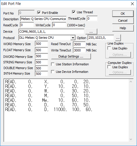
<Figure 1> is read setting example of Melsec Q Series CPU communication driver.
|
|
| <Figure 1> Read setting example of Melsec Q Series CPU communication driver |
Device part of <Figure 1> input com port(COM6), baud rate(9600), data bit(8), stop bit(1) respectively, accordint to the setting of controller.
In protocol option part, you can set the following: PC No.(255 or 1 ~ 64), Destination Module I/O No.(single PLC : 1023, ... ), Destination Module Station No.(default = 0). Each argument is a comma-delimited.
PC No. : 255 or 1 ~ 64,
Destination Module I/O No. : single – 1023 (03FFh),
PLC 1 - 992 (03E0h), PLC 2 – 993 (03E1h), PLC 3 - 994 (03E2h), PLC 4 – 995 (03E3h),
Multi Drop connection – 0 ~ 511 (01FF).
Destination Module Station No. : single – 0,
Multi Drop connection – 0 ~ 31 (01F).
Read schedule of Melsec Q Series CPU communication driver
Read schedule setting parameters are as follows:
1) station – fixed to 0.
2) read memory – B, CC, CCw, CN, CS, CSw, D, DX, DY, F, Fw, L, Lw, M, Mw, R, S, S w, SB, SC, SCw, SD, SM, SMw, SN, SS, SSw, SW, TC, TCw, TN, TS, TSw, V, Vw, W, X, Y, Z, ZR.( refer to <Table 1> ).
3) read start address – read start address. ( X, Y, B, ... memory = read start address x 16 )
4) Save start address for Communication Server – Saving start address of Communication Server.
5) Read size – read size. word, 10bit unit : 1 ~ 490, double word, Float : 1 ~ 245
Read schedule example)
READ, 0, X, 0, 0, 20,
READ, 0, Y, 10, 20, 10,
READ, 0, W, 0, 30, 20,
READ, 0, M, 0, 50, 10,
READ, 0, Mw, 10, 60, 10,
READ, 0, D, 0, 70, 50,
READ, 0, D, 11000, 100, 60,
<Table 1> is Memory type and contensts of MELSEC Q Series PLC.
| Memory type | Contents | Bit write | Read/Write command | read unit | Address | Remarks |
| B | LINK relay | O | B | WORD | hex-decimal | * read size = 1 word unit = 16 bit(1 word ), 10bit unit = 10 bit Digital write for CN, D, R, TN, W = bit operation after word unit reading. |
| CC | Counter | O | CC | 10 BIT | decimal | |
| CCw | WORD | |||||
| CN | X | CN | WORD | |||
| CS | O | CS | 10 BIT | |||
| CSw | WORD | |||||
| D DD2 DF2 |
DATA register | X | D DD2 DF2 |
WORD DWORD FLOAT |
||
| DX | Direct Input | O | DX | WORD | hex-decimal | |
| DY | Direct Output | DY | WORD | |||
| F | ANNUNCIATOR | O | F | 10 BIT | decimal | |
| Fw | WORD | |||||
| L | LATCH relay | O | L | 10 BIT | ||
| Lw | WORD | |||||
| M | Internal relay | O | M | 10 BIT | ||
| Mw | WORD | |||||
| R | FILE register | X | R | WORD | ||
| S | STEP relay | O | S | 10 BIT | ||
| S w | WORD | |||||
| SB | Special Link relay | O | SB | WORD | hex-decimal | |
| SC | Retentive Timer | O | SC | 10 BIT | decimal | |
| SCw | WORD | |||||
| SN | X | SN | WORD | |||
| SS | O | SS | 10 BIT | |||
| SSw | WORD | |||||
| SD | Special register | X | SD | WORD | ||
| SM | STEP relay | O | SM | 10 BIT | ||
| SMw | WORD | |||||
| SW | Special LINK register | O | SW | WORD | hex-decimal | |
| TC | Timer | O | TC | 10 BIT | decimal | |
| TCw | WORD | |||||
| TN | X | TN | WORD | |||
| TS | O | TS | 10 BIT | |||
| TSw | WORD | |||||
| V | EDGE relay | O | V | 10 BIT | ||
| Vw | WORD | |||||
| W | LINK register | X | W | WORD | hex-decimal | |
| X | Input relay | O | X | WORD | ||
| Y | Output relay | Y | WORD | |||
| Z | INDEX register | X | Z | WORD | decimal | |
| ZR | FILE register(Serial NO. Access) | O | ZR | WORD | hex-decimal | |
| <Table 1> Memory type and contensts of MELSEC Q Series PLC | ||||||
If you click the icon ![]() in protocol option part at
<Figure 1>, you
can see the dialog box such as <Figure 2>. you can also set read schedule by
using this part.
in protocol option part at
<Figure 1>, you
can see the dialog box such as <Figure 2>. you can also set read schedule by
using this part.
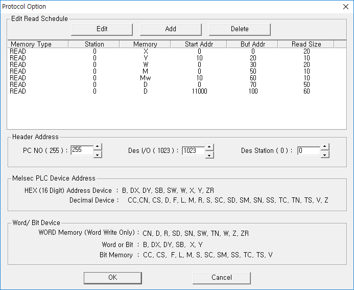 |
| <Figure 2> Example of Melsec Q Series CPU communication driver’s Option dialog box |
You can set read schedule by using
![]() ,
,
![]() ,
,
![]() button and listbox of <Figure
2>.
button and listbox of <Figure
2>.
Also, you can set set PC No., Destination Module I/O No., Destination Module Station No. by using the part of 'PC NO', 'DES I/O', 'Des Station' shown in <Figure 2>.
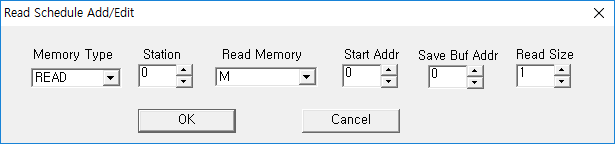 |
| <Figure 3> Example of Melsec Q Series CPU communication driver’s read schedule Add/Edit dialog box |
When you click Add button or Edit button in dialogue box of <Figure 2>, dialogue box of <Figure 3> is shown.
You can set Melsec PLC by using 'writing settings'.
Digital Write
Digital write setting parameters are as follows:
( CN, D, R, SD, SN, SW, TN, W, Z, ZR = bit operation after word unit reading )
1) PORT Port no. (0 ~ 255)
2) STATION station number of PLC. ( single PLC = 0 )
3) ADDRESS address in PLC memory.
B, DX, DY, SB, SW, W, X, Y, ZR = hex-decimal unit,
other = decimal unit.
4) Extra1 write memory type = B, CC, CN, CS, D, DX, DY, F, L, M, R, S, SB, SC, SD, SM, SN, SS, SW, TC, TN, TS, V, W, X, Y, Z, ZR.
5) Extra2 don't care.
Write example 1)
PORT: 0, station: 0, ADDRESS:001A, Extra1: Y, Extra2 : 0
The setting parameter shown above is bit control(On/Off) example for Y001A address ( bit unit ) of Y memory.
Write example 2)
PORT: 0, station: 0, ADDRESS: 0100, Extra1: M, Extra2 : 0
The setting parameter shown above is bit control(On/Off) example for 100 address ( bit unit ) of M memory.
Analog Write
Analog write setting parameters are as follows:
1) PORT Port no. (0 ~ 255)
2) STATION station number of PLC. ( single PLC = 0 )
3) ADDRESS address in PLC memory.
B, DX, DY, SB, SW, W, X, Y, ZR = hex-decimal unit,
other = decimal unit. ( CC, CS, F, L, M, S, SC, SM, SS, TC, TS, V : bit memory = 16 bit write )
4) Extra1 write memory type = B, CC, CN, CS, D, DX, DY, F, L, M, R, S, SB, SC, SD, SM, SN, SS, SW, TC, TN, TS, V, W, X, Y, Z, ZR.
5) Extra2 block write option.
0, space : normal Analog write,
1 : output value and address saving for block(multi) write,
2 : sequential block write by using saved data, ( maximum block write count = 256)
3 : random block write by using saved data,
4 : delete all saved data for block write.
Write example 1)
PORT: 0, station: 0, ADDRESS: 0015, Extra1: D, Extra2 : 0
The setting parameter shown above is word write example for D0015 address( word unit ) of D memory.
Write example 2)
PORT: 0, station: 0, ADDRESS: 000A, Extra1: Y, Extra2 : 0
The setting parameter shown above is word write example for Y000A address ( word unit ) of Y memory.