LG SV-IS5 communication driver is the driver to communicate with inverter of LSIS Co., Ltd. in Korea.
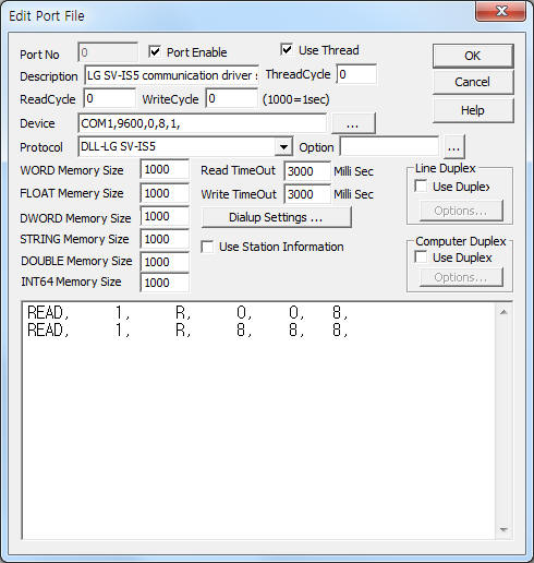
<Figure 1> is read setting example of LG SV-IS5 communication driver.( LS BUS protocol )
 |
| <Figure 1> Read setting example of LG SV-IS5 communication driver |
Device part of <Figure 1> input Com Port(COM1), Baud Rate(9600), Parity Bit(0), Data Bit(8), Stop Bit(1) respectively, according to controller.
Baud rate(1200,2400,4800,9600,19200bps), Parity bit(0, 1, 2), Data bit, Stop bit(1, 2) of SV-IS5 can set operation button of Inverter.
LG SV-IS5 communication driver read schedule
1) Station – 1 ~ 31 station number of inverter.
2) Read command – Command.
R – read of common area data, ( ( refer to <table 1> , <Table 2> or manual of SV-IS5 )
Y – read of relay status(Digital Input) value.
3) Read start address – Address of SV-iS5. ( 0 ~ )
4) Save start address for Communication Server – Saving start address of Communication Server.
5) Read Size – 1 ~ 8 read size.
Read schedule example)
READ, 1, R, 0, 0, 8,
READ, 1, R, 8, 8, 8,
<Table 1> is address range of each group data.
<Table 2> is address range and contents for common area.
Note) Please refer to manual of SV-IS5 for DRV, FU1, FU2, I/O, EXT, COM, APP, ...
Group |
Range of address |
Remarks |
common area |
0x0000 ~ 0x0015 |
refer to <Table 2> |
DRV |
0x5100 ~ 0x510A |
refer to manual of SV-IS5 |
FU1 |
0x5203 ~ 0x523C |
|
FU2 |
0x5307 ~ 0x535D |
|
I/O |
0x5401 ~ 0x5431 |
|
EXT |
0x5501 ~ 0x552B |
|
COM |
0x5601 ~ 0x5603 |
|
APP |
0x5701 ~ 0x5721 |
|
| <Table 1> Address range of each group data | ||
| Address | Contents | R/W | Rnage |
| 0x0000 | model of inverter | R | 4 = SV-iS5 |
| 0x0001 | capacity of inverter | 0 = 0.75, 1 = 1.5, 2 = 2.2, 3 = 3.7, 4 = 5.5, 5 = 7.5, 6 = 11, 7 = 15, 8 = 18.5, 9 = 22, A = 30, B = 37, C = 45, D = 55, E = 75, F = 90, 10 = 110, 11 = 132, 12 = 160, 13 = 200, 14 = 220, 15 = 280, 16 = 375. (unit : KW) |
|
| 0x0002 | input voltage of inverter | 0 = 220V, 1 = 440V, ... |
|
| 0x0003 | version | 0100 : Ver 1.00, 0101 : Ver 1.01 |
|
| 0x0004 | - | - | - |
| 0x0005 | frequency assignation | R/W | 0.01 HZ |
| 0x0006 | operation assignation | Bit 0 : stop, Bit 1 : forward run, Bit 2 : reverse run, Bit 3 : Fault reset, Bit 4 : emergency stop |
|
| 0x0007 | acceleration time | 0.1 Sec |
|
| 0x0008 | deceleration time | ||
| 0x0009 | output current | R | 0.1 A |
| 0x000A | output frequency | 0.01 HZ |
|
| 0x000B | output voltage | 0.1 V |
|
| 0x000C | DC Link voltage | ||
| 0x000D | output power | 0.1 KW |
|
| 0x000E | operation status | Bit 0 : stop, Bit 1 : forward run, Bit 2 : reverse run, Bit 3 : Fault (Trip), Bit 4 : accelerating, Bit 5 : decelerating, Bit 6 : reached speed, Bit 7 : DC Breaking, Bit 8 : stopping, Bit 9 : don't use, Bit 10 : break open, Bit 11 : forward assignation, Bit 12 : reverse assignation, Bit 13 : Rem. Run/Stop, Bit 14 : Rem. Freq.Cord. |
|
| 0x000F | trip information | Bit 0 : OCT1, Bit 1 : OV, Bit 2 : EXT-A, Bit 3 : BX, Bit 4 : OCT2, Bit 5 : GF, Bit 6 : OH, Bit 7 : ETH, Bit 8 : OLT, Bit 9 : HW-ding, Bit 10 : EXT-B, Bit 11 : FO, Bit 12 : OPT, Bit 13 : PO, Bit 14 : IOLT, Bit 15 : LV. |
|
| 0x0010 | input connector information | Bit 0 ~ 5 : P1 ~ P6, Bit 6 : RST, Bit 7 : BX, Bit 8 : JOG, Bit 9 : FX, Bit 10 : RX. |
|
| 0x0011 | output connector information | Bit 0 : Q1(OC1), Bit 1 : Q1(OC2), Bit 2 : Q3(OC3), Bit 3 : AUX, Bit 4 : 30AC. |
|
| 0x0012 | V1 | 0 ~ FFC0 |
|
| 0x0013 | V2 | ||
| 0x0014 | I | ||
| 0x0015 | RPM | ||
| <Table 2> Address range and contents for common area | |||
If you click the icon
![]() in protocol option part, you can see the dialog
box such as <Figure 2>. you can also set read schedule by using this part.
in protocol option part, you can see the dialog
box such as <Figure 2>. you can also set read schedule by using this part.
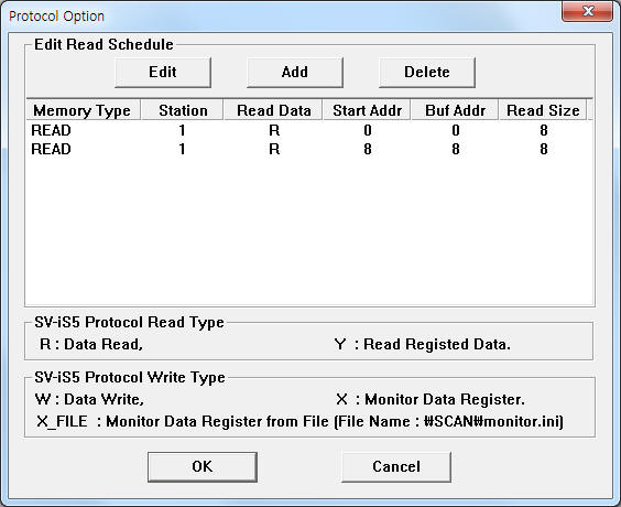 |
| <Figure 2> Example of LG SV-IS5 communication driver’s Option dialog box |
You can set read schedule by using
![]() ,
,
![]() ,
,
![]() button and listbox of <Figure 2>.
button and listbox of <Figure 2>.
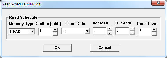 |
| <Figure 3> Example of LG SV-IS5 communication driver’s read schedule Add/Edit dialog box |
When you click Add button or Edit button in dialogue box of <Figure 2>, dialogue box of <Figure 3> will be shown.
You can set LG SV-IS5 controller by using 'writing settings'.
LG SV-IS5 controller can write only R/W address.
Digital write
Digital write setting parameters are as follows:
1) PORT Port no. (0 ~ 255)
2) STATION 1 ~ 31 station number of inverter.
3) ADDRESS writing address. ( hex-decimal unit )
W write command : higher 3 digit – address of inverter, lower 1 digit - 0 ~ F bit position,
X write command : 4digit address to be registered,
X_FILE write command : don't care.
4) Extra1 write command.
W : Bit unit write command,
X : single data Address Monitor register,
X_FILE : multi data(max = 8) Address Monitor register, the setting data read at 'work folder\SCAN\monitor.ini' file.
5) Extra2 don't care.
Write example 1)
PORT:0, station:1, ADDRESS:0061, Extra1:W, Extra2 : 0
The setting parameter shown above is forward run(On/Off) control example of 1 SV-IS5 inverter.
Write example 2)
PORT:0, station:1, ADDRESS:0012, Extra1:X, Extra2 : 0
The setting parameter shown above is single data Address Monitor register example of 12 address.
Write example 3)
PORT:0, station:1, ADDRESS:0000, Extra1:X_FILE, Extra2 : 0
The setting parameter shown above is multi data Address Monitor register example. Setting register data read from 'work folder\SCAN\monitor.ini' file.
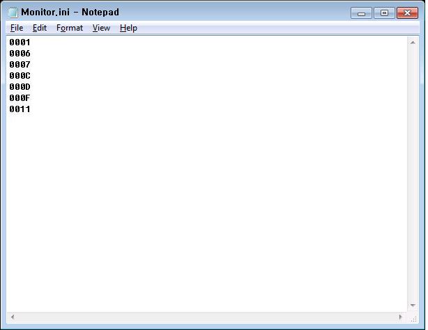 |
| <Figure 4> Example of Address Monitor register file |
Analog Write
Analog write and digital write have the same setting parameters except output value and address. ( address = 4 digit hex-decimal unit address of inverter )
Write example 1)
PORT:0, station:1, ADDRESS:0007, Extra1:W, Extra2 : 0
The setting parameter shown above is acceleration time setting example of 1 SV-IS5 inverter.
Write example 2)
PORT:0, station:1, ADDRESS:0008, Extra1:W, Extra2 : 0
The setting parameter shown above is deceleration time setting example of 1 SV-IS5 inverter.
Connection of communication cable and setting of station, baud rate are as follows.
Connection of communication cable
Please connect 2, 3, 8 pin of 10pin socket and 3, 2, 5 pin of computer(RS-232C 9pin socket such as <Figure 5>.
SV-IS5 inverter computer (9pin socket)
pin 2(up-right->2nd from left) ---------------------- pin 3
pin 3(up-right->3rd from left) ---------------------- pin 2
pin 8(up-right->8th from left) ---------------------- pin 5
Setting of station and baud rate
Station and baud rate of SV-IS5 inverter can set operation button of Inverter. ( refer to <Figure 6> )
<Figure 6> is appearance of SV-IS5 inverter.
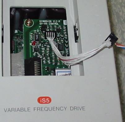 |
| <Figure 5> Connection example between SV_IS5 inverter and computer |
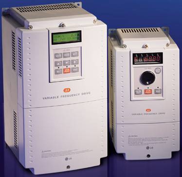 |
| <Figure 6> Appearance of SV-IS5 inverter |
<Figure 7>, <Figure 8> are model, wiring of SV-IS5 inverter.
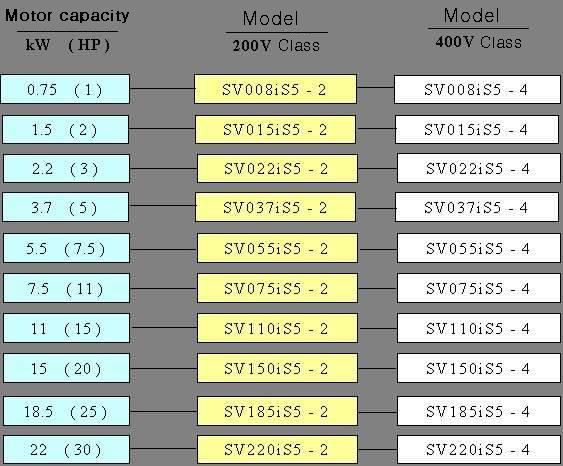 |
| <Figure 7> Model of SV-IS5 inverter |
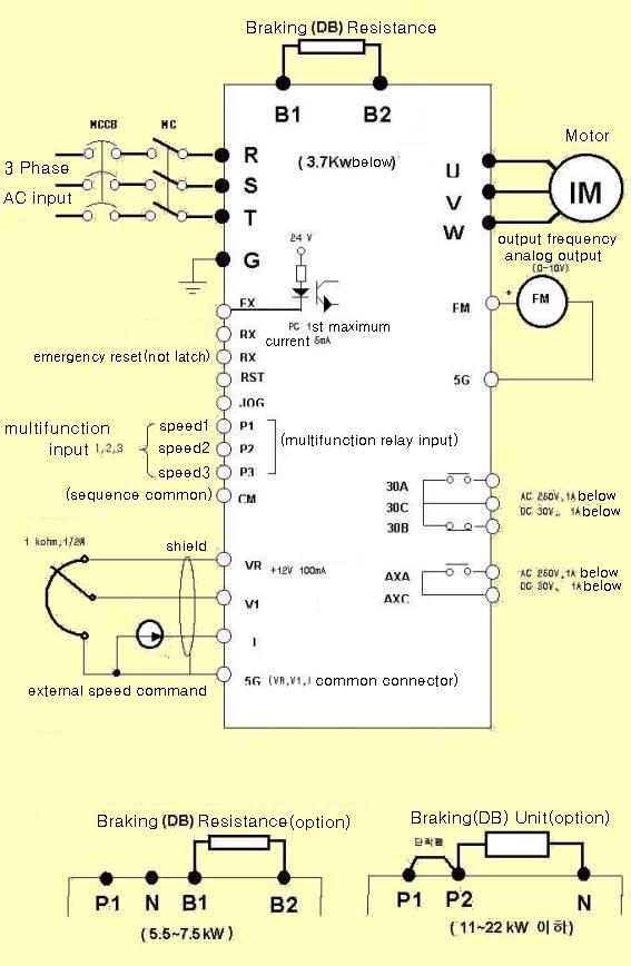 |
| <Figure 8> Wiring of SV-IS5 inverter |
<Table 3> is specification of SV-IS5 inverter.
2 0 0 V class |
Specification | SV008 iS5-2 |
SV015 iS5-2 |
SV022 iS5-2 |
SV037 iS5-2 |
SV055 iS5-2 |
SV075 iS5-2 |
SV110 iS5-2 |
SV150 iS5-2 |
SV185 iS5-2 |
SV220 iS5-2 |
||||||||
| maximum applicable motor | [HP] | 1 | 2 | 3 | 5 | 7.5 | 10 | 15 | 20 | 25 | 30 | ||||||||
| [kW] | 0.75 | 1.5 | 2.2 | 3.7 | 5.5 | 7.5 | 11 | 15 | 18.5 | 22 | |||||||||
| rated output | rated capacity[kVA] | 1.9 | 3.0 | 4.5 | 6.1 | 9.1 | 12.2 | 17.5 | 22.9 | 28.2 | 33.5 | ||||||||
| rated current[A] | 5 | 8 | 12 | 16 | 24 | 32 | 46 | 60 | 74 | 88 | |||||||||
| output frequency | 0 ~ 400 Hz | ||||||||||||||||||
| output voltage | 200 ~ 230 V | ||||||||||||||||||
| rated input | voltage | 3 phase 200 ~ 230 V (± 10 %) | |||||||||||||||||
| frequency | 50 ~ 60 Hz (± 5 %) | ||||||||||||||||||
| inverter weight(kg) | 4.6 | 4.6 | 4.8 | 4.9 | 7.5 | 7.7 | 13.8 | 14.3 | 19.4 | 20 | |||||||||
4 0 0 V class |
model | SV008 iS5-4 |
SV015 iS5-4 |
SV022 iS5-4 |
SV037 iS5-4 |
SV055 iS5-4 |
SV075 iS5-4 |
SV110 iS5-4 |
SV150 iS5-4 |
SV185 iS5-4 |
SV220 iS5-4 |
||||||||
| maximum applicable motor | [HP] | 1 | 2 | 3 | 5 | 7.5 | 10 | 15 | 20 | 25 | 30 | ||||||||
| [kW] | 0.75 | 1.5 | 2.2 | 3.7 | 5.5 | 7.5 | 11 | 15 | 18.5 | 22 | |||||||||
| rated output | capacity[kVA] | 1.9 | 3.0 | 4.5 | 6.1 | 9.1 | 12.2 | 18.3 | 22.9 | 29.7 | 34.3 | ||||||||
| rated current[A] | 2.5 | 4 | 6 | 8 | 12 | 16 | 24 | 30 | 39 | 45 | |||||||||
| output frequency | 0 ~ 400 Hz | ||||||||||||||||||
| output voltage | 380 ~ 460 V | ||||||||||||||||||
| rated input | voltage | 3 phase 380 ~ 460 V (± 10 %) | |||||||||||||||||
| frequency | 50 ~ 60 Hz (± 5 %) | ||||||||||||||||||
inverter weight(kg) |
4.7 | 4.7 | 4.8 | 4.9 | 7.7 | 7.7 | 13.9 | 14.4 | 20 | 20 | |||||||||
control |
control method | selection of V/F control, sensorless vector control | |||||||||||||||||
| frequency setting resolution |
digital command : 0.01Hz (under 100Hz), 0.1Hz (more
than 100Hz) analog command : 0.06Hz/60Hz analog command : 0.03 Hz / 60 Hz |
||||||||||||||||||
| frequency precision | digital : 0.01 % of maximun output frequency analog : 0.1 % of maximun output frequency analog : 0.1 % of maximun output frequency |
||||||||||||||||||
| V/F ratio | linear, squared, User V/F | ||||||||||||||||||
| overload capacity | 150 % 1 minute,200% 0.5 second (inverse time characteristics) | ||||||||||||||||||
| torque boost | manual torque boost(0 ~ 15% setting), automatic torque boost | ||||||||||||||||||
run |
run method | selection of key / connector / communication run | |||||||||||||||||
| frequency setting | analog : 0 ~ 10V/4 ~ 20 mA/auxiliary
when using sub-board(0 ~ 10V) |
||||||||||||||||||
| input signal | run signal | forward rotation,reverse rotation | |||||||||||||||||
| multi-step selection | setting enable maximum 8 (use multifunction connector) | ||||||||||||||||||
| multi-accel/decel time selection | 1 ~ 6,000 second, setting
enable each 8 type, selection enable (use multifunction connector) |
||||||||||||||||||
| emergency stop | Instantaneous stop(block) of inverter output | ||||||||||||||||||
| jog | jog run | ||||||||||||||||||
| automatic run | internal sequence operation according to selection of multifunction connector(5 way * 8 step) | ||||||||||||||||||
| abnormal reset | release trip status when operating protection function | ||||||||||||||||||
| output signal | run status | frequency detection,overload warning,in stall,over-voltage,low-voltage,overheat
of inverter,running,stoping,constant speed, etc switching common usage,searching of speed,automatic operation step,automatic operation sequence |
|||||||||||||||||
| abnormal output | relay(contact) output(30A,30C,30B) - AC250V 1A,DC30V 1A | ||||||||||||||||||
| indicator | 1 selection among output frequency,output
current,output voltage,DC voltage, pulse output 500Hz, output voltage 0 ~ 10V |
||||||||||||||||||
| function of run | DC braking,frequency limit,frequency jump,2nd
function,slip compensation, reverse rotation prevention, automatic re-start,switching common usage,auto-tuning,PID control |
||||||||||||||||||
protection function |
inverter trip | over-voltage,low-voltage,over-current,fuse open,ground
fault protection,overheat of inverter,overheat of motor,input/output phase
loss, etc over-load protection,external out of order 1,2,communication error,los of speed command,abnormal of hardware,abnormal of option, etc |
|||||||||||||||||
| inverter warning | stall protection,over-load warning, abnormal of temperature sensor | ||||||||||||||||||
| instantaneous power failure | 15 msec below: continuous operation, 15 msec over: enable automatic re-start | ||||||||||||||||||
|
display |
loader | run information | output frequency,output current,output voltage,frequency setting value,operation(run) speed,DC voltage | ||||||||||||||||
| trip information | display abnormal status when operating protection function,save 5 trip information at system | ||||||||||||||||||
|
operating environment |
ambient temperature | -10 ℃ ~ 40 ℃ | |||||||||||||||||
| storage Temperature | -20 ℃ ~ 65 ℃ | ||||||||||||||||||
| ambient humidity | relative humidity 90 % RH below(should not dewing situation) | ||||||||||||||||||
| altitude, vibration | 1,000 m below · 5.9m/sec²(=0.6g) below | ||||||||||||||||||
| ambient environment | should not causticity gas,flammable gas,oil mist,dust, etc in indoors | ||||||||||||||||||
| cooling method | forced cooling | ||||||||||||||||||
| protection structure | closed type(IP20) | ||||||||||||||||||
| <Table 3> Specification of SV-IS5 inverter | |||||||||||||||||||