FUJI MICREX-F ENET communication driver is the driver to communicate with ethernet module PLC((120S ~ 150S, 120H ~ 150H) of Fuji Electric Co., Ltd. in Japan.
Note) For communicate with ethernet module of FUJI MF series PLC, you have to make Ladder routine for setting of ethernet communication.
Reference : PLC setting for using FUJI MICREX-F ENET communication driver
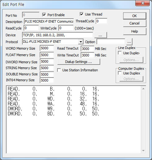
<Figure 1> is read setting example of FUJI MICREX-F ENET communication driver.
 |
| <Figure 1> Read setting example of FUJI MICREX-F ENET communication driver |
Device part of <Figure 1> input Device type(TCP/IP or UDP/IP), IP address of PLC(192.168.0.2), service port of TCP/IP(UDP/IP) protocol (2000 ),respectively, according to setting of PLC.
Note) When a communication error about TCP/IP connection occurs, the problem can be solved as follows.
1) Make 2 or more TCP/IP (or UDP/IP) service port routine in the Ladder program.
2) Input service port number at 'Device' part of <Figure 1> such as 2000, 2011, 2002 …(service port number = made by ladder program).
3) It can slove TCP/IP connection problem by connecting the next service port.
FUJI MICREX-F ENET communication driver read schedule
Read schedule setting parameters are as follows:
1) STATION – Don't care.
2) Read command – Read memory type or command = B, M, K, F, A, D, W9, TS, TR, CS, CR, BD, WL, WL2, WB, Wm, WK, WA, WD, W21. ( Refer to <Table 1>, <Table 2> )
3) Read start address – Read start address in memory type = 0 ~ .
4) Save Start Address for Communication Server – saveing start address of Communication Server.
5) Read Size – Read size of Byte,Word, Dword unit = Byte : 1 ~ 212, Word 1 ~ 106, Dword : 1 ~ 53.
Read schedule example)
READ, 0, B, 0, 0, 16,
READ, 0, M, 0, 16, 16,
READ, 0, WD, 0, 32, 16,
READ, 0, WA, 0, 48, 16,
DWORD, 0, W9, 0, 0, 50,
DWORD, 0, BD, 0, 50, 50,
<Table 1> is memory type and data form of FUJI MICREX-F ENET communication driver.
<Table 2> is memory type and read/write command of FUJI MICREX-F ENET communication driver.
| Memory type | Data form | Remarks |
B |
WORD |
Digital input/output area |
M |
WORD |
Internal memory area |
K |
WORD |
|
F |
WORD |
|
A |
WORD |
|
D |
WORD |
|
W9 |
DWORD |
|
TS |
DWORD |
|
TR |
DWORD |
|
CS |
DWORD |
|
CR |
DWORD |
|
BD |
DWORD |
|
WL |
WORD |
Bit type of WL memory area |
WB |
BCD_WORD |
Get 16 bit BCD value at B memory area |
WM |
BCD_WORD |
Get 16 bit BCD value at M memory area |
WK |
BCD_WORD |
Get 16 bit BCD value at K memory area |
WF |
BCD_WORD |
Get 16 bit BCD value at F memory area |
WA |
BCD_WORD |
Get 16 bit BCD value at A memory area |
WD |
BCD_WORD |
Get 16 bit BCD value at D memory area |
| <Table 1> Memory type and data form of FUJI MICREX-F ENET communication driver | ||
| Device Memory type | Contents | Read/Write command | Address range (when 120S : decimal) | Remarks |
| B | Input, output relay | B | 0 ~ 511 | Bit Address, WORD unit |
| WB | WORD | |||
| M | Auxiliary relay | M | Bit Address, WORD unit | |
| WM | WORD | |||
| K | Keep relay | K | 0 ~ 63 | Bit Address, WORD unit |
| WK | WORD | |||
| F | Special relay | F | 0 ~ 125 | Bit Address, WORD unit |
| WF | WORD | |||
| A | Annunciate relay | A | 1 ~ 45 | Bit Address, WORD unit |
| WA | WORD | |||
| D | Differential relay | D | 0 ~ 63 | Bit Address, WORD unit |
| WD | WORD | |||
| S | Step control | WS | 0 ~ 99 | BYTE ( 8 Bit ) |
| W9 | Current value of 0.1second timer | W9 | 0 ~ 511 | DWORD |
| TS | Setting value of timer | TS | ||
| TR | Current value of timer | TR | ||
| CS | Setting value of counter | CS | ||
| CR | Current value of counter | CR | ||
| BD | Data memory | BD | 0 ~ 255 | |
| WL | 0 station 1 block memory of P-Link memory | WL | 0 ~ 4095 | WORD |
| W21 | 0 station 2 block memory of P-Link memory | W21 | ||
| W22 | 0 station 3 block memory of P-Link memory | W22 | ||
| W23 | 0 station 4 block memory of P-Link memory | W23 | ||
| W24 | Direct input, output I/O | W24 | 0 ~ 127 | |
| W25 | Analog work area | W25 | 0 ~ 511 | DWORD |
| W26 | Old value of differential relay | W26 | 0 ~ 63 | WORD |
| W120 | 1 station 1 block memory of P-Link memory | W120 | 0 ~ 4095 | |
| W121 | 1 station 2 block memory of P-Link memory | W121 | ||
| W122 | 1 station 3 block memory of P-Link memory | W122 | ||
| W123 | 1 station 4 block memory of P-Link memory | W123 | ||
| W125 | Calendar area | W125 | 0 ~ 5 | |
|
|
||||
| W30 ~W109 | File memory | FILE30 ~ 109 | 0 ~ 4095 | WORD |
| FILED30 ~ 109 | DWORD | |||
| <Table 2> Memory type and read/write command of FUJI MICREX-F ENET communication driver | ||||
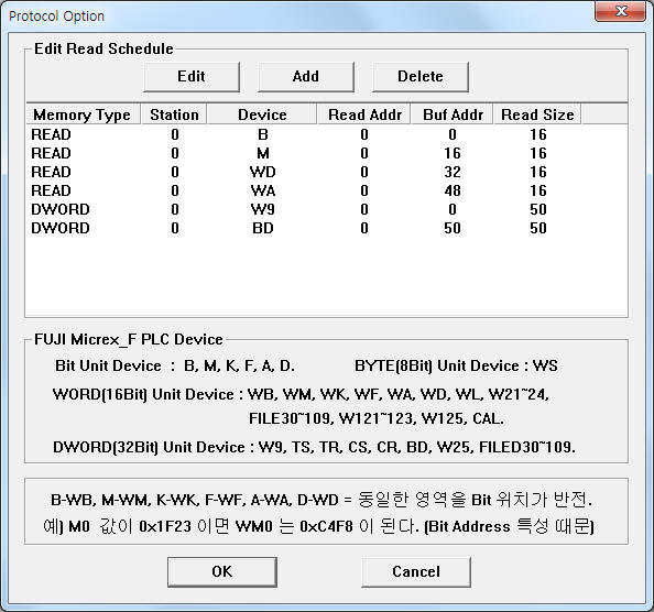
If you click the icon ![]() in protocol option part, you
can see the dialogue box such as <Figure 2>. you can also set read schedule by
using this part.
in protocol option part, you
can see the dialogue box such as <Figure 2>. you can also set read schedule by
using this part.
 |
| <Figure 2> Example of FUJI MICREX-F ENET communication driver’s Option dialogue box |
You can set read schedule by using ![]() ,
, ![]() ,
, ![]() button and listbox of <Figure
2>.
button and listbox of <Figure
2>.
 |
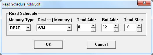
| <Figure 3> Example of FUJI MICREX-F ENET communication driver’s read schedule Add/Edit dialogue box |
When you click Add button or Edit button in dialogue box of <Figure 2>, dialogue box of <Figure 3> is shown.
You can change the value of device memory by using write settings.
Digital Write
Digital write setting parameters are as follows:
1) PORT Port no. (0 ~ 255)
2) STATION Don't care.
3) ADDRESS Write addres in memory type.
Byte unit device memory(WS, ...) : higher 3 ~ 7 digit = byte unit address, lower 1 digit = 0 ~ 7 bit position,
Word unit device memory : higher 3 ~ 7 digit = word unit address, lower 1 digit = 0 ~ F bit position,
Dword unit device memory : higher 3 ~ 7 digit = dword unit address, lower 1 digit = 0 ~ F bit position, 10h ~ 1Fh bit position = value of Extra2(0 ~ 1).
4) Extra1 Write memory type = B, WB, M, WM, K, WK, F, WF, A, WA, D, WD, WS, W9, TS, TR, CS, CR, BD, WL, W21, W22, W23, W24, W25, W26, FILE30 ~ 109, FILED30 ~ 109, W120, W121, W122, W123, W125, CAL (Refer to <Table 2>)
5) Extra2 Higher bit position when Dword unit device memory.
W9, TS, TR, CS, CR, BD, W25,... Dword device memory : 0 = 0h ~ Fh bit position, 1 = 10h ~ 1Fh bit position,
other device memory : don't care.
Note) Word, Dword unit device memory don't support digital(bit) unit write protocol.
So FUJI FC Series CCS communication driver made digital write by 'bit operation method' after reading the word, dword memory.
When the 'digital output', B-WB, M-WM, K-WK, F-WF, A-WA, D-WD device memory equal area, but bit position is opposite such as <Table 3>.
(B, M, K, F, A, D Device memory's bit address and word address have inverse bit position)
Example) M0 = 1F23h, WM0 = C4F8h
Normally Digital read/wirite use B, M, K, F, A, D command, Analog read/wirite use WB, WM, WK, WF, WA, WD command.
| Device type | Bit position | |||||||||||||||
| WB, WM, WK, WF, WA, WD,... | 0 | 1 | 2 | 3 | 4 | 5 | 6 | 7 | 8 | 9 | A | B | C | D | E | F |
| B, M, K, F, A, D,... | F | E | D | C | B | A | 9 | 8 | 7 | 6 | 5 | 4 | 3 | 2 | 1 | 0 |
| <Table 3> Bit position acoording to device type | ||||||||||||||||
Write example 1)
PORT:0, station:0, ADDRESS:001A, Extra1: M, Extra2 :
The setting parameter shown above is a bit write(On/Off) example of M001A(A bit, 1 word) in the M device memory.
Write example 2)
PORT:0, station:0, ADDRESS:0100, Extra1: M, Extra2 :
The setting parameter shown above is a bit write(On/Off) example of M0100(0 bit, 10 word) in the M device memory.
Write example 3)
PORT:0, station:0, ADDRESS:012F, Extra1: BD, Extra2 : 0
The setting parameter shown above is a bit write(On/Off) example of F(16th) bit, 12(13th) dword in the BD device memory.
Write example 4)
PORT:0, station:0, ADDRESS:012F, Extra1: BD, Extra2 : 1
The setting parameter shown above is a bit write(On/Off) example of 1F(32th) bit, 12(13th) dword in the BD device memory.
Analog Write
Analog write setting parameters are as follows:
1) PORT Port no. (0 ~ 255)
2) STATION Don't care.
3) ADDRESS Word unit addres in memory type.
4) Extra1 Write memory type = B, WB, M, WM, K, WK, F, WF, A, WA, D, WD, WS, W9, TS, TR, CS, CR, BD, WL, W21, W22, W23, W24, W25, W26, FILE30 ~ 109, FILED30 ~ 109, W120, W121, W122, W123, W125, CAL (Refer to <Table 2>)
5) Extra2 Don't care.
Write example 1)
PORT:0, station:0, ADDRESS:0000, Extra1: WM, Extra2 :
The setting parameter shown above is an word write example of 0(1st) word in the M device memory.
Write example 2)
PORT:0, station:0, ADDRESS:0015, Extra1: WD, Extra2 :
The setting parameter shown above is an word write example of 15(16th) word in the D device memory.
Write example 3)
PORT:0, station:0, ADDRESS:0031, Extra1: BD, Extra2 :
The setting parameter shown above is an double word write example of 31(32th) double word in the BD device memory.
Write example 3)
PORT:0, station:0, ADDRESS:0125, Extra1: W9, Extra2 :
The setting parameter shown above is an double word write example of 125(126th) double word in the W9 device memory.